Nvidia's latest release of the "GPU" DGX-2, consisting of 16 V100+12 NVSwitch chips, provides 2 PFLOPS. The single V100 Deep Learning processing capability is 120TFLOPS. If we want to design an AI chip that can achieve 40PFLOPS processing capability, what should I do? In fact, it is quite "simple" to make the chip area as large as possible. What is the maximum size of a single die? Of course, it is the area of ​​a Wafer. This is the topic to be discussed today, Wafer Scale Integration (WSI). This is not a fantasies. It is said that someone is trying an 8 inch x 8 inch WSI. The indicator it achieves is 40 PFLOPS and consumes 17 kW (16 nm process). This article is not intended to discuss the rumors, but to explore the possibility of WSI. After all, previous attempts have failed. There is a sense of image, I drew a 1:1 ratio of this chip on the A4 paper Die (Italian 41290.24mm2). Everyone can feel it, almost A4 paper can not let go. As a comparison also draws Nvidia's P100 chip Die (Assuming it is a square) (area is 610mm2). This is compared with P100 because it is also a 16nm process. The classmates who made the chips should all understand what a single wafer produces for only one die, so when I posted this map to a circle of friends it also attracted fierce comments. In addition to asking who this is, the problems are mainly related to yield, fault tolerance, packaging, and heat dissipation. Of course, everyone's questions have come up with ideas. Like the systolic arrays we discussed previously (Pulsing Arrays - New to Google TPU), and asynchronous circuits (whether "legendary" asynchronous circuits can rise in the AI ​​chip?), WSI is not new. The history of Wikipedia's "Wafer-scale integration" can be seen. In the 70s and 80s of the last century, there have been a lot of attempts in this area. Its goal is mainly to serve the massively parallel supercomputers. If it can be realized, the benefits are obvious, and a large number of computing and storage resources can be realized on a single chip, and the communication between them can use relatively inexpensive "on the cheap" connection resources on the chip. However, all attempts at that time failed. At the 1984 ISSCC meeting, there was a discussion about WSI. One of the organizers was David A. Patterson. The following description of the problem can be seen in the minutes of the meeting: The 60s, various approaches were tried, first to reduce system cost. Then, the scale of integration was too low and the ratio of redundant circuits to active circuits was too high to be cost-effective compared to more direct means of improving yield. Today, there are several additional motivations for wafer scale integration/redundancy including: system reliability; high performance through the use of very wide, fast data busses for array/systolic processors and CPUs; and system flexibility and reconfigurability. The major issues for application of WSI include generality; technical problems such as testing and yield statistics; and practical problems such as packaging, ruggedness, repairability, and system partitioning. In the following discussion, there is an optimistic view that a practical WSI system can be realized with the advancement of related chip technologies in the next five years; there are also pessimistic arguments that it can never be the mainstream chip technology. Although we can hardly predict the future, at least so far the latter is more accurate. As mentioned earlier, the biggest WSI challenges include two aspects. The first is the technical problems associated with the defects introduced in silicon wafer production. Then comes the actual problems faced in the integration, including packaging, cooling, power supply and so on. Let us first look at the former. For fault-tolerant design, there is a lot of exploration and experience in chip design, and some are quite mature. We can find many references for possible errors and fixes (including hardware and software fixes) in operations, storage, and interconnections. Taking into account some of the characteristics of the AI ​​chip, fault-tolerant design may be relatively easy to handle some. First, the proportion of memory in the AI ​​chip is high, and the fault-tolerant design of the memory is a mature technology. Second, taking into account the characteristics of AI algorithms, both DNN and brain-like computing (SNN) are likely to do some fault-tolerant design at the algorithm level. ([2] can also see the description of this) Third, AI chips generally use a more regular multi-core architecture (connected with NoC), in WSI can be more naturally divided into different areas (similar to a virtual on Wafer "Segmentation" into many dies. In this way, even if there are defects that cannot be repaired by software, it can be partially solved by sacrificing performance and shutting down an independent kernel. Among the various defects, the most troublesome is the short circuit problem. Once the power supply is short-circuited, the entire area will hang. The possibility of a short circuit to the power source is still quite cumbersome. This point does not know if there is a good way. Another problem is the uniformity of the process. It is difficult to ensure that the device performance in the entire wafer area is consistent with the high-end process. This may lead to inconsistent performance in different regions and inconsistent core speeds between the wafer center and the edge. In this case, the inter-chip interconnection needs special processing, and system operation and scheduling are also very challenging. Some fault-tolerant designs need to be built on the basis of positioning defects. Only by accurately locating the defects can they be repaired. If it is a synchronous design, basically the existing DFT method has little problem, mainly the scale of the test. In addition, a large number of functional tests should be performed in time, requiring a relatively long time for testing, repair and debugging. However, chips of this size must be sold systematically, and even if more debugging time is needed, it is not a problem. Of course we can't be 100% fault tolerant in practice, but the final consideration is still economical, ie how much to pay (such as redundant chip area, performance loss, etc.) to prevent, test and repair defects can be economically Accepted. This part of the topic is quite numerous, and there are opportunities for further discussion.
DIP Sockets & Adapters
Precision machined Dual In-line Package (DIP) Sockets and Adapters accommodate applications from surface mount to thru-hole. Screw-machined terminals offer superior quality for long-term durability. DIP Sockets Adapters,DIP Integrated circuit Sockets,Dual In-line Package Sockets,Dual In-line Package Adapters,IC Socket, IC Sockets Adapters ShenZhen Antenk Electronics Co,Ltd , https://www.antenkconn.com
Although it is an outspoken technique, I believe that when people see such indicators as 40PFLOPS, they will still be interested in doing more in-depth analysis. In fact, for the first time, when I heard that a company was doing this thing, it basically did not believe it. Until it was confirmed from many sides, it began to think seriously about its possibilities. 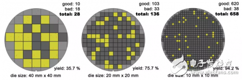
Defects must occur during chip production. Defects should appear on the wafer with different probabilities depending on the complexity of the process. Mean defect density D0. In general chip production, a lot of dies are cut from a single wafer. For chips that are defective and cannot be "repaired", the elimination is fine. With the same defect distribution, the larger the die on the wafer (the smaller the number of splits), the greater the effect of the defect (the area to be rejected is approximately larger). The figure above is a reflection of the relationship between yield and die area. For the extreme case of WSI such as a wafer and a die, if the rejection is the entire wafer is wasted. So, if you only look at one Wafer, we can say that its yield is '0%'. WSI's yield rate should look at the proportion of all Wafer chips that work properly (or almost normal). It is not difficult to see that the challenge of WSI is mainly how to minimize the impact of mistakes, that is, fault-tolerant design issues, when there are bound to be errors.
Overview of DIP Sockets & Adapters
DIP Sockets and Adapters allow for quick and easy device replacement, upgrade, or repair in test and production applications, while protecting DIP devices from exposure to heat during board processing. Screw-machined terminals with redundant, multi-finger contacts ensure reliable performance even in harsh environments.
Automated assembly compliant.
Wide range of patterns and terminal styles, from 8 to 64 pins.
Optional Tape Seal on terminals protects contacts from contaminants during board processing.
Solder Preform terminals available for mixed SMT and thru-hole process applications.
RoHS Compliant insulators and terminals are compatible with lead-free processing - select either Matte Tin/Gold (MG) or Gold/Gold (GG) plating.
Our large selection of DIP sockets ranging from 1 to 48 contacts can provide a highly reliable connection between your integrated circuit (IC) devices and PCBs. Antenk offers DIP sockets in a wide variety for high reliability. Positions range from 1 to 48, and termination options include through hole and surface mounting, solderless zero profile, four-finger inner contact and dual leaf contacts, as well as a variety of plating options.

Antenk DIP Sockets Product Features
1 to 48 positions
Precision four-finger inner contacts or dual leaf contacts are optional
Open frame and closed frame housings
Available with a variety of plating options
Four-Fingered Contacts
Precision machined or stamped four-finger inner contacts with open or closed frame housings facilitate highly reliable DIP sockets.
Dual Leaf Contacts
Dual leaf contacts provide a cost effective solution to the DIP socket design with superior handling characteristics.
How to design a 40PFLOPS AI chip_Operation process
Antenk DIP (Dual Inline Package) Sockets-Classic DIP Sockets